How Should Thermal Silicone Pads Be Designed for 800G and 1.6T Optical Modules?
- Share
- publisher
- SiliconePlus Engineering Team
- Issue Time
- Sep 16,2026
Summary
Thermal silicone pad design for 800G and 1.6T optical modules depends on more than thermal conductivity. Pad thickness, compression, hardness, contact area, assembly stack-up, heat-spreader flatness, dimensional tolerance and cleanliness all affect thermal and mechanical performance. This guide explains what engineers should define before tooling, sampling and mass production.
Answer Excerpt
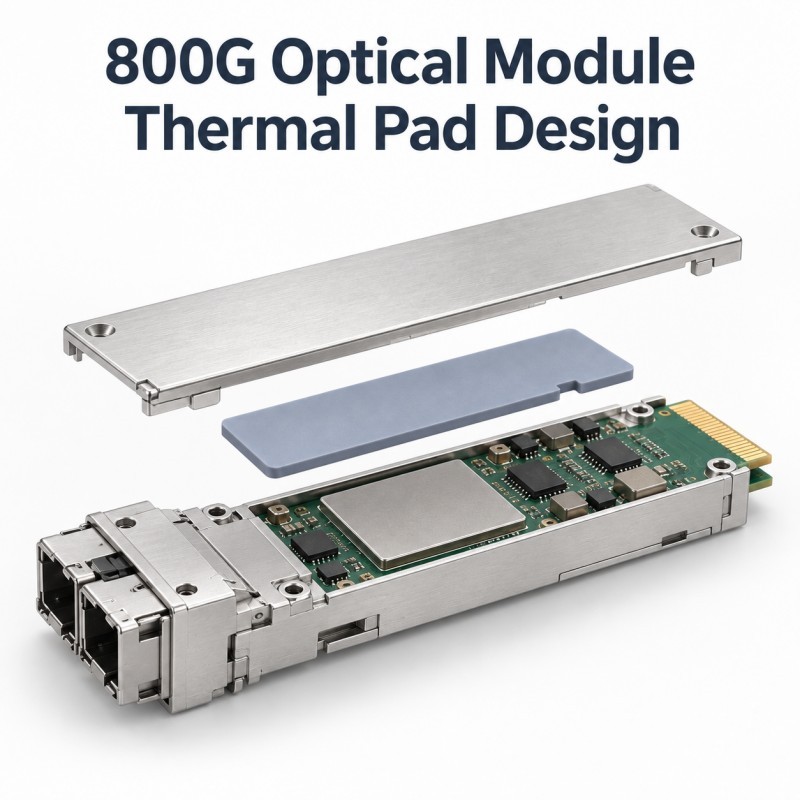
A thermal silicone pad for an 800G or 1.6T optical module should be designed as part of the complete thermal and mechanical stack-up rather than selected only by thermal conductivity.
The pad must create stable contact between heat-generating components and the heat spreader while accommodating small gaps, component-height variation and mating-surface tolerance. At the same time, it should not create excessive compression force on the PCB, optical engine or other sensitive components.
Key design variables include thermal conductivity, pad thickness, compression range, silicone hardness, contact area, heat-spreader flatness, electrical insulation requirements, cleanliness, dimensional tolerance and long-term compression recovery.
The final design should be validated in the actual optical module assembly rather than from the thermal pad alone.
Where Is a Thermal Silicone Pad Used in an Optical Module?
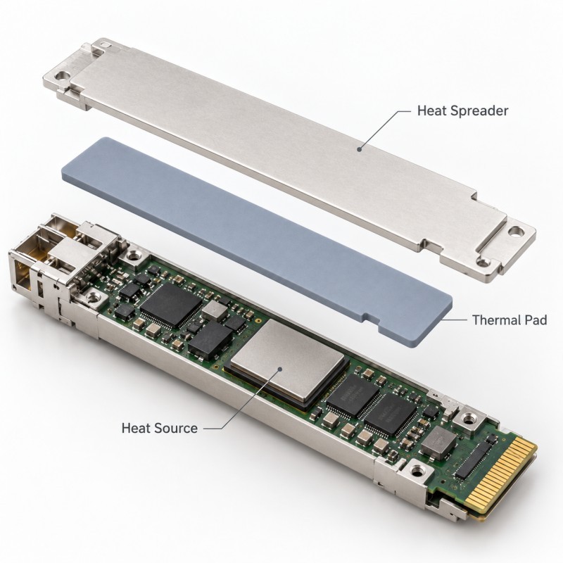
High-speed optical transceivers integrate heat-generating electronics into a very limited mechanical envelope.
Depending on the module architecture, a custom thermal silicone pad may be positioned between a heat-generating component and a metal heat spreader, module housing or another cooling structure.
Typical thermal-interface locations may include:
• DSP or processing-device thermal interfaces
• Driver or electronic component interfaces
• PCB heat-source areas
• Heat-spreader contact zones
• Local component groups with different heights
• Other defined thermal contact areas inside the module
The purpose of the silicone pad is not simply to cover the electronics.
It should fill the intended interface gap and create a controlled heat-transfer path while leaving optical, electrical and mechanical functional areas correctly exposed.
The pad should never be allowed to interfere with the optical path, connector interface, screw locations, alignment features or other functional areas of the transceiver.
Why Can Small Air Gaps Become a Thermal Problem?
A heat source and a metal heat spreader may appear to contact each other in CAD, but the real assembly can contain small gaps.
These gaps may result from:
• Component-height tolerance
• PCB flatness variation
• Heat-spreader flatness
• Housing tolerance
• Surface roughness
• Assembly gap variation
• Local component positioning
• Fastener or clip conditions
If a rigid metal surface cannot maintain continuous contact with the heat-generating area, part of the interface may contain air.
A compliant thermal silicone pad can deform into these small variations and create more continuous contact.
However, the pad must also remain thin enough and compressed correctly enough to avoid adding unnecessary thermal resistance.
This is why optical module thermal management should be reviewed as a complete assembly stack-up rather than by choosing a pad from a material data sheet alone.
1. Thermal Conductivity Is Important—but It Is Not the Only Specification
Thermal conductivity is usually one of the first specifications discussed when selecting an optical module thermal pad.
However, a higher conductivity value does not automatically guarantee a lower component temperature in the final module.
Actual performance also depends on:
• Pad thickness
• Real contact area
• Compression condition
• Interface flatness
• Surface contact
• Heat-source size
• Heat-spreader design
• Assembly pressure
• Material consistency
For example, a material with a high conductivity value may still perform poorly if the pad is unnecessarily thick or does not maintain continuous contact with both mating surfaces.
The correct material grade should therefore be selected according to the customer's thermal requirement and validated in the complete module.
SiliconePlus does not assume one fixed thermal conductivity value for every optical module project. The target should be defined by the customer's design and selected material grade.
2. Pad Thickness Must Match the Real Assembly Stack-Up
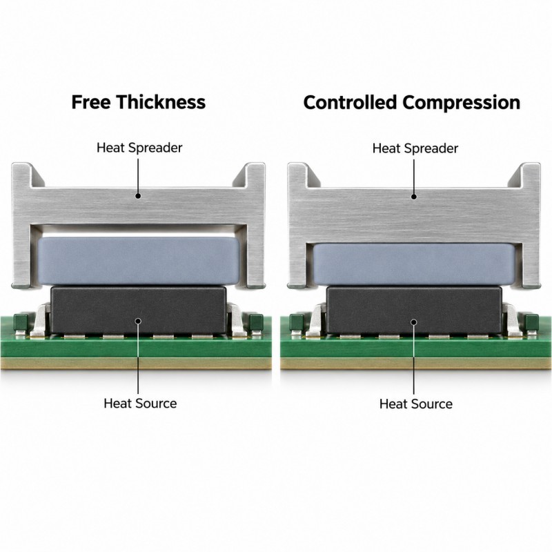
Thermal pad thickness should not be selected independently from the module geometry.
The required thickness depends on the distance between the heat-generating surface and the heat spreader after the complete module is assembled.
Engineers should review:
• Minimum interface gap
• Nominal interface gap
• Maximum interface gap
• Component-height variation
• Heat-spreader tolerance
• PCB position
• Housing tolerance
• Pad dimensional tolerance
• Final compression condition
If the pad is too thin, part of the thermal interface may not make reliable contact.
If the pad is unnecessarily thick, the thermal path becomes longer and the silicone may require greater deformation during assembly.
The thickness specification should therefore come from the real mechanical stack-up—not from a standard pad thickness chosen before the module structure is reviewed.
3. Compression Must Improve Contact Without Overloading Sensitive Components
A thermal silicone pad needs enough compression to conform to the mating surfaces and maintain contact.
But maximum compression is not the design objective.
Excessive compression can increase mechanical load on:
• PCB assemblies
• Solder joints
• Electronic packages
• Optical assemblies
• Heat-spreader structures
• Module housings
Insufficient compression may create:
• Partial surface contact
• Local air gaps
• Unstable thermal resistance
• Greater sensitivity to tolerance variation
• Inconsistent performance between assemblies
The target should therefore be a controlled compression window that provides reliable contact without creating unnecessary mechanical stress.
Compression should be reviewed at minimum, nominal and maximum stack-up conditions.
4. Silicone Hardness Affects Contact and Assembly Force
Silicone hardness affects how easily the thermal pad conforms to the heat source and heat spreader.
A softer material may:
• Deform more easily
• Conform to small surface variations
• Require lower compression force
But excessive softness can also make handling, dimensional stability and assembly control more difficult.
A firmer silicone may:
• Maintain its shape more effectively
• Improve handling stability
• Resist excessive local deformation
But it may require greater force to achieve the required interface contact.
Hardness should therefore be evaluated together with pad thickness, compression space, contact area and the mechanical strength of the module assembly.
The final decision should be made from molded samples and real assembly testing rather than from Shore hardness alone.
5. Contact Area Should Follow the Real Heat-Source Layout
A custom thermal pad does not always need to be one simple rectangle.
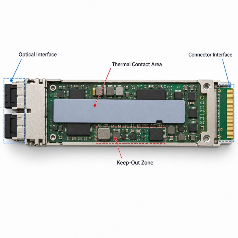
The pad outline can be developed according to the actual heat-source layout and available interface area.
Depending on the module structure, custom geometry may include:
• Local cutouts
• Edge notches
• Different contact zones
• Rounded corners
• Defined keep-out areas
• Stepped or localized geometry where manufacturable
The purpose is to place thermal-interface material only where it supports the intended heat-transfer path.
The pad should not unnecessarily cover areas that do not require thermal contact.
For precision optical modules, this becomes especially important because a small product envelope may contain heat-generating electronics, optical structures, connector interfaces, mounting features and other functional zones in very close proximity.
6. Optical Paths and Connector Interfaces Must Remain Clear
Thermal management should never be designed by ignoring the optical and electrical functions of the module.
Before the pad outline is finalized, engineers should identify all areas that must remain free from silicone.
These may include:
• Optical paths
• Optical engine keep-out areas
• Connector interfaces
• Electrical contacts
• Screw holes
• Locating features
• Mechanical datums
• Module latches or moving structures
• Service or inspection areas
A thermal pad should contact only the intended heat-transfer surfaces.
For custom molded pads, these boundaries should be clearly defined on the 2D drawing and 3D model before tooling.
This reduces the risk of a pad interfering with assembly or covering a functional area that must remain accessible.
7. Flatness and Tolerance Stack-Up Affect Real Pad Compression
The nominal CAD gap is not necessarily the gap that exists in every production module.
Actual compression may change because of:
• Heat-spreader flatness
• PCB flatness
• Component-height tolerance
• Housing dimensions
• Fastener position
• Assembly force
• Pad thickness tolerance
• Molded pad dimensional variation
A design that works perfectly at the nominal dimension may create insufficient contact at one tolerance extreme and excessive compression at the other.
For this reason, DFM should evaluate minimum, nominal and maximum stack-up conditions.
Critical pad dimensions should also have a clearly defined inspection method because flexible silicone can deform during measurement.
8. Electrical Insulation and Cleanliness Requirements Should Be Defined Early
Optical modules combine thermal, electrical and optical functions in a compact package.
Depending on the actual application, the thermal pad project may also need to define:
• Electrical insulation requirement
• Surface cleanliness
• Particle-control requirement
• Material traceability
• Color or identification requirement
• Surface condition
• Packaging cleanliness
• Handling requirements
Cleanliness is particularly important when a silicone component is installed near sensitive optical or electronic structures.
Foreign particles, oil, release residue or loose contamination may create problems even if the pad itself meets its dimensional specification.
The customer should therefore define any application-specific cleanliness or electrical requirements before material and process approval.
9. Thermal Cycling and Long-Term Compression Can Change the Interface
An optical module thermal pad may remain compressed for long periods while repeatedly experiencing changes in operating temperature.
Over time, the complete thermal interface may be affected by:
• Silicone compression recovery
• Heat-spreader expansion
• PCB movement
• Housing expansion and contraction
• Repeated thermal cycling
• Material aging
• Assembly stress
The initial assembly condition should therefore not be the only validation point.
The project may need to confirm whether the pad maintains sufficient contact after the defined temperature and aging conditions.
The exact validation method should be based on the customer's real module requirement rather than one generic test condition.
| Design Item | Why It Matters | Main Risk | What to Validate |
Thermal conductivity | Supports heat transfer | Material chosen by datasheet only | Module thermal result |
Pad thickness | Determines thermal path and gap filling | Too thin or unnecessarily thick | Assembly stack-up |
Compression | Creates interface contact | Low contact or excessive stress | Min/nominal/max condition |
Hardness | Affects conformity and force | Poor contact or excessive load | Assembly force |
Contact area | Defines thermal interface | Missing or unnecessary coverage | Heat-source layout |
| Flatness | Changes local contact | Local air gap | Heat spreader and PCB |
| Tolerance | Changes real compression | Unit-to-unit inconsistency | Worst-case stack-up |
| Cleanliness | Protects sensitive assembly | Particle contamination | Inspection standard |
10. How Should an Optical Module Thermal Pad Be Validated?
A custom thermal pad should be validated in the actual optical module assembly or in a representative engineering fixture.
The validation plan may include:
1. Dimensional Inspection
Confirm overall outline, thickness, cutouts, notches and other critical molded dimensions.
2. Assembly Fit Check
Confirm that the pad aligns correctly with the intended heat source and does not interfere with connectors, optical structures or fastening features.
3. Compression Evaluation
Confirm the pad reaches the intended compressed condition across the realistic assembly tolerance range.
4. Thermal Validation
Evaluate the thermal result using the customer's defined test method, power condition, temperature points and acceptance criteria.
5. Mechanical Load Review
Confirm that pad compression does not create excessive force on sensitive components or the PCB.
6. Thermal Cycling or Aging
Where required, repeat functional evaluation after the specified environmental or aging condition.
7. Cleanliness Inspection
Confirm the pad and packaging meet the defined contamination-control requirements.
8. Pilot Production
Validate multiple consecutive parts rather than approving production from only one engineering sample.**
The goal is not simply to make one thermal pad that fits.
The goal is to produce stable geometry and repeatable interface performance across production batches.
What Should Be Included in an RFQ for an Optical Module Thermal Pad?
For a more accurate engineering review and quotation, the customer should provide as much of the following information as possible:
• 2D drawing
• 3D CAD model
• Optical module type or assembly structure
• Heat-source location
• Heat-spreader geometry
• Required pad outline
• Target pad thickness
• Minimum and maximum assembly gap
• Compression requirement
• Thermal conductivity target
• Silicone hardness requirement if already defined
• Electrical insulation requirement
• Operating temperature
• Cleanliness requirement
• Thermal validation requirement
• Estimated annual or order quantity
• Physical samples when available
If the material grade has already been approved by the customer, that information should also be provided.
If it has not yet been defined, the required thermal and mechanical performance should be provided instead of assuming one standard material.
How SiliconePlus Supports Custom Optical Module Thermal Pads
SiliconePlus supports custom molded silicone components based on the customer's drawing, application structure and functional requirements.
For optical module thermal pad projects, engineering support can include:
• Drawing and DFM review
• Pad outline and contact-area review
• Thickness and stack-up evaluation
• Silicone hardness review
• Customer-specified thermal material selection
• Custom molded geometry
• Mold development
• Dimensional inspection
• Sample development
• Pilot production
• OEM/ODM mass production support
The product should be developed around the actual module structure instead of forcing one standard thermal pad into every design.
For projects with custom cutouts, notches, controlled thickness or non-standard geometry, molding feasibility should be reviewed before tooling.
FAQ
What Does a Thermal Silicone Pad Do in an Optical Module?
A thermal silicone pad creates a compliant interface between a heat-generating component and a heat spreader or cooling structure. It helps accommodate small gaps and surface variation while maintaining thermal contact under controlled compression.
Is Higher Thermal Conductivity Always Better for an Optical Module Pad?
Not by itself. Final thermal performance also depends on pad thickness, compression, contact area, surface flatness, assembly pressure and the complete module thermal path. The material grade should be selected according to the customer's actual thermal target.
How Should Thermal Pad Thickness Be Selected?
Thickness should be determined from the real assembly stack-up, including the minimum, nominal and maximum gap between the heat-generating surface and the heat spreader. A standard thickness should not be selected before the mechanical stack-up is reviewed.
Can a Thermal Pad Be Too Compressed?
Yes. Excessive compression can increase mechanical load on the PCB, electronic packages, optical structures or housing. The objective is controlled interface contact rather than maximum compression.
Can an Optical Module Thermal Pad Have Custom Cutouts and Notches?
Yes, where the molding process and geometry allow it. Custom outlines, notches, openings and contact zones can be developed according to the heat-source layout, assembly clearance and functional keep-out areas.
What Information Is Needed to Quote a Custom 800G Optical Module Thermal Pad?
Provide the 2D/3D drawing, module stack-up, heat-source location, heat-spreader structure, pad thickness, compression requirement, thermal target, operating temperature, material requirements and estimated order quantity.
Conclusion
A thermal silicone pad for an 800G or 1.6T optical module should not be selected from thermal conductivity alone.
Reliable interface performance depends on the combined control of:
• Thermal material grade
• Pad thickness
• Compression
• Silicone hardness
• Heat-source contact area
• Heat-spreader flatness
• Mechanical stack-up
• Dimensional tolerance
• Electrical requirements
• Cleanliness
• Thermal cycling and aging conditions
The thermal pad must fill the intended gap without creating unnecessary mechanical load or interfering with optical, electrical or mechanical functions.
The best time to define these requirements is during DFM and module stack-up review—before the pad tooling and material specification are finalized.
Developing an 800G or 1.6T Optical Module Thermal Interface?
If you are developing a custom thermal silicone pad for an 800G, 1.6T, OSFP, QSFP-DD or other optical transceiver assembly, send your 2D/3D drawing, heat-source layout, heat-spreader structure, target thickness, compression condition, thermal requirement and estimated quantity to the SiliconePlus engineering team.
We can review pad geometry, stack-up, molding feasibility, dimensional requirements and sampling conditions before mold development and mass production.
For thermal material properties such as thermal conductivity, the final value should be defined according to the selected material grade and your project validation requirements.