How Should PCB Support and Component Clearance Be Designed for LSR Overmolding?
- Share
- publisher
- SiliconePlus Engineering Team
- Issue Time
- Oct 23,2026
Summary
LSR overmolding can protect PCB and FPC assemblies, but the board, mounted components and silicone coverage boundary must be designed as one system. This guide explains board support, component clearance, tooling considerations, process compatibility and validation requirements to review before tooling begins.
Answer Excerpt
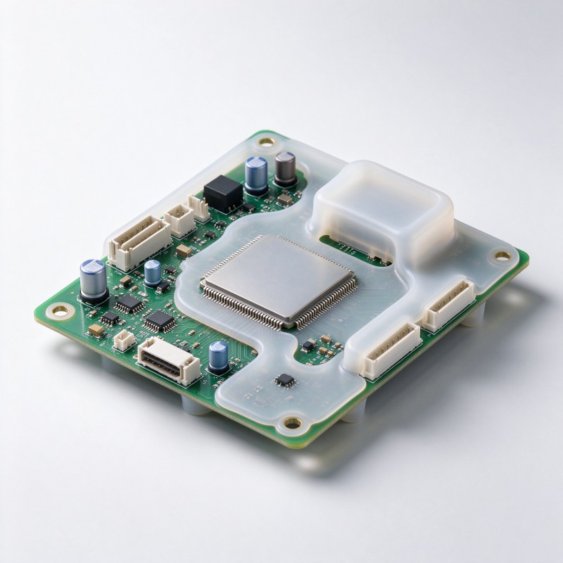
LSR overmolding a PCB or FPC assembly requires more than choosing a silicone cover shape. The board must be supported at defined rigid datums, component height and clearance must be mapped in three dimensions, and the intended silicone coverage boundary must be separated from sensitive components and functional interfaces. Unsupported spans, uneven support, board thickness variation and the molding cycle can affect positioning or assembly integrity. Before tooling, engineers should review the complete populated board, confirm process compatibility with the actual components and define post-molding dimensional and functional checks. The final protection level must be validated on the assembled design; it cannot be inferred from the presence of silicone alone.
Why Does PCB Support Matter During LSR Overmolding?
A PCB assembly is not necessarily a rigid, uniform insert. Its behavior depends on board thickness, outline, cutouts, mounted components, connectors, stiffeners and the locations available for support.
During LSR overmolding, the assembly is located and held in a tooling system while the silicone is introduced and cured. If the board is not adequately supported, an unsupported area may deflect or move. Even without visible damage, movement can change the intended silicone boundary, alter local coverage or affect the position of functional features.
Potential risks include:
- Board deflection or movement during mold closing and filling
- Unintended loading on mounted components, solder joints or connectors
- Variation in silicone coverage caused by inconsistent board positioning
- Damage to components that contact an unintended support or tooling surface
- A mismatch between the molded cover and the final housing assembly
These risks should be evaluated against the actual board design and process conditions rather than assumed to occur in every project.
For a product-specific reference, review the custom LSR-overmolded PCB silicone cover offered by SiliconePlus. The actual coverage, board support and component-clearance requirements must be established from the customer's assembly drawings and application needs.
What Board and Component Information Should Be Defined Before Tooling?
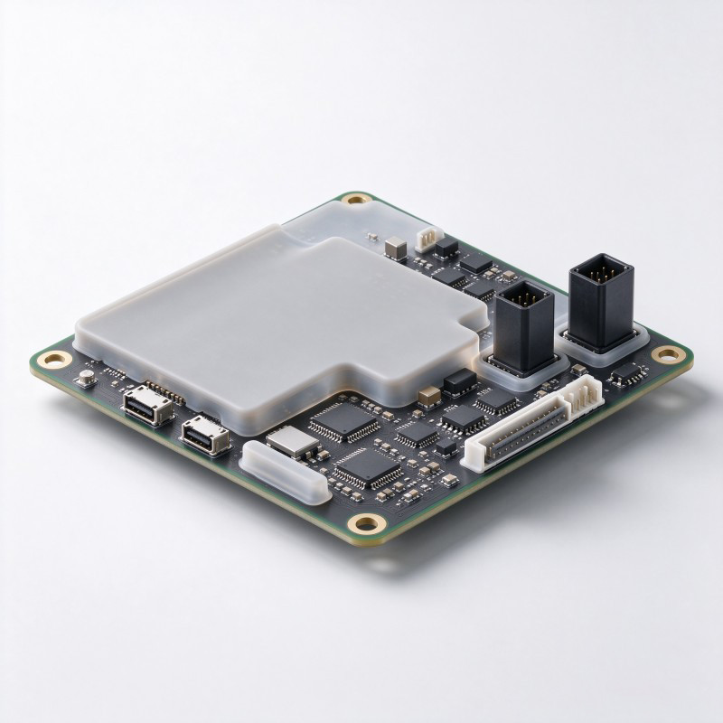
Before tooling, the engineering team should review the complete PCB or FPC assembly rather than a simplified board outline alone.
The information package should identify:
- Board outline, thickness and relevant dimensional tolerances
- PCB stack-up or FPC construction, including any stiffeners where applicable
- The location and maximum height of mounted components
- Connector, switch, sensor and other interface locations
- Areas that may receive silicone and areas that must remain uncovered
- Available rigid datums and suitable board-support locations
- Components or assembly materials with defined process-exposure limits
- The required electrical, mechanical and environmental functions after molding
A three-dimensional assembly model is particularly useful when component heights, connector positions and the proposed silicone cover overlap in the same region. If a complete 3D model is unavailable, the buyer should provide sufficiently detailed drawings and component-height information for a meaningful feasibility review.
Where a flexible circuit is involved, evaluate the full assembly rather than treating the FPC as a single uniform sheet. Silicone coverage, local reinforcement, support and the actual circuit construction need to be considered together. SiliconePlus also provides FPC silicone overmolding solutions for drawing-based customization.
The objective is to establish a shared definition of the board, components, support areas and silicone coverage before mold design begins.
PCB Overmolding Inputs and Why They Matter
| Design input | What to define | Why it matters |
Board outline | External profile, cutouts and critical dimensions | Establishes the locating and support strategy |
Board thickness | Nominal thickness and permitted variation | Affects seating, support and clearance |
Component envelope | Component locations and maximum heights | Helps prevent unintended contact or loading |
Support datums | Approved rigid reference and support areas | Improves insert-position repeatability |
Silicone coverage | Intended overmold boundary and local geometry | Defines which areas receive protection |
| Protected areas | Components and interfaces that must remain accessible or untouched | Prevents functional interference |
| Process limits | Exposure limits for the actual board assembly | Supports process-compatibility review |
| Acceptance criteria | Required dimensional and functional checks | Makes sample approval objective and repeatable |
How Should the Board Be Supported Inside the Tool?
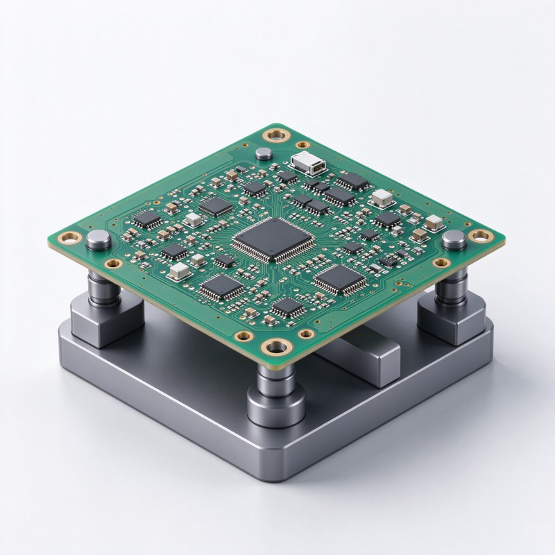
Board support should be designed around stable, approved locations on the actual assembly. The goal is to keep the board correctly positioned without applying unintended loads to fragile components or functional interfaces.
A practical support review should consider the following points.
Use repeatable locating references. The tooling concept should identify the rigid features that control the board's position. The location strategy should not depend on an operator judging the board position by eye.
Reduce uncontrolled unsupported spans. Where the board outline or cutouts create flexible regions, review whether additional support is needed. Support locations must suit the actual board structure and must not interfere with components or the intended silicone coverage.
Avoid loading sensitive components. Components, solder joints, connectors and other populated features should not become accidental locating points unless the assembly design explicitly allows that load.
Account for board variation. Board thickness, flatness, outline and component placement can vary within the approved specification. The support concept should be reviewed against these variations, not only a nominal CAD model.
Check the complete molding sequence. Board positioning must remain stable during loading, mold closing, silicone filling, curing and demolding. The appropriate support and process conditions depend on the real assembly and tooling design.
The required support method and process conditions must be established through engineering review and sample evaluation. They should not be selected from a generic pressure or temperature value.
For projects that require process-specific review, SiliconePlus provides liquid silicone injection molding services for custom components based on drawings and application requirements.
How Should Silicone Coverage and Component Clearance Be Defined?
The silicone coverage boundary should be defined against the complete board assembly, not only the two-dimensional PCB outline.
Engineers should identify which regions require silicone protection, which regions need clearance, and which features must remain available for electrical connection, assembly, adjustment or service.
Three-dimensional review is important because a component can sit outside the intended silicone footprint in a top view while still conflicting with the cover height or a nearby transition.
The review should address:
- The intended overmolded region and its relationship to the board outline
- Component height and lateral position near the coverage boundary
- Clearance between the silicone structure and components that must remain uncovered
- Connector and mating-interface access after molding
- Changes in silicone thickness or geometry around local board features
- The relationship between the molded cover and the final housing or mounting structure
Do not assume that the entire PCB should be encapsulated. Depending on the product architecture, localized overmolding may be more appropriate when components or interfaces must remain accessible.
The clearance requirement should be determined from the real geometry, dimensional variation, tooling concept and application requirements. There is no single universal clearance value that can safely be applied to every PCB assembly.
The approved drawing should clearly distinguish the silicone coverage boundary from component-clearance zones. Those requirements should then be checked during sample inspection and final assembly evaluation.
Component Zones and Design Controls
| Assembly zone | Design control | Inspection focus |
Intended silicone coverage | Define the permitted overmold area | Coverage boundary and molded geometry |
Tall components | Define component envelope and required clearance | Unintended contact, loading or interference |
Connectors and mating interfaces | Mark access and assembly requirements | Connector access and final fit |
Sensitive electronic components | Identify process and mechanical limitations | Visible damage and required functional checks |
| Board locating areas | Define approved support datums | Position repeatability and board condition |
| Silicone transitions | Review local thickness and boundary geometry | Uneven coverage or interference with adjacent features |
| Final housing interface | Provide mating geometry where available | Assembly fit and required sealing function |
How Should Thermal Exposure and Assembly Loads Be Reviewed?
A PCB assembly must be suitable for the actual molding process, not just for the silicone material in isolation.
Before approving tooling, the engineering team should review the specified process exposure against the limits of the board assembly and its mounted components. Depending on the design, relevant items may include connectors, component packages, soldered joints, bonded layers, surface finishes and other materials that form part of the assembly.
The review should establish:
- Which components or materials have restricted process-exposure conditions
- Whether the proposed molding and curing sequence is compatible with the assembled board
- Whether support and clamping could create unintended mechanical loads
- Whether the proposed silicone structure could interfere with the final housing
- Which component functions need to be checked after molding
Do not assume that every electronic component is compatible with every LSR process. Suitability depends on the actual component specifications, board construction and agreed process conditions.
The mold concept should also be reviewed for locating references, support surfaces, coverage boundaries, clearance and demolding feasibility. Review the proposed arrangement against SiliconePlus' silicone mold design capabilities before the tooling design is finalized.
Where a design contains bonded FPC stiffeners or other adhesive-dependent layers, those structures require their own compatibility assessment. Board support and component clearance are related but distinct from adhesive-bond integrity.
The final process window and acceptance criteria should be agreed for the actual project and confirmed during sample evaluation.
How Should the Finished Assembly Be Validated?
Validation should examine both the molded silicone structure and the PCB assembly that remains underneath it.
A useful project plan can include the following checks, selected according to the product's actual requirements.
Board condition and position. Inspect the assembly for visible damage, unintended movement or changes in the relevant board dimensions.
Silicone coverage and clearance. Confirm that the molded boundary matches the approved drawing and that the intended component-clearance zones remain clear.
Component condition. Check for visible damage, displacement or other abnormalities in areas identified as sensitive during the design review.
Electrical and functional checks. Where electrical performance is critical, define suitable checks before and after molding. The specific tests should reflect the circuit's intended function.
Final assembly fit. Where the PCB is installed into a housing or another assembly, check the relevant mating interfaces and installation requirements.
Environmental or protection validation. If the project requires moisture protection, sealing, vibration resistance or other environmental performance, define the test method and acceptance criteria with the product owner. A silicone cover alone does not prove a particular protection rating.
Production repeatability. Once the sample design is approved, confirm that the agreed inspection method can be applied consistently to production parts.
The validation plan should be defined before sample approval. Test results, protection ratings and acceptance claims must be based on actual testing against the agreed criteria, not on assumptions from the design concept.

What Should Buyers Include in an RFQ?
For an accurate feasibility review and quotation, buyers should provide enough information to define the complete board assembly and the intended silicone protection.
A useful RFQ package includes:
- 2D drawings and, where available, a 3D model of the PCB/FPC assembly
- Board outline, thickness, relevant tolerances and construction details
- Component locations and maximum component heights
- Connector and mating-interface information
- The required silicone coverage area and any areas that must remain uncovered
- Available board-support datums or fixture references
- Known thermal, mechanical or material limitations of the assembled electronics
- The required protection function and the actual operating environment
- Final housing or mating-part drawings, where applicable
- Required dimensional, electrical, assembly and environmental validation
- Prototype quantity, estimated production quantity and project schedule
If the board includes components with restricted process exposure, identify them before tooling. If the cover must fit into a separate housing, provide the mating geometry rather than evaluating the silicone part in isolation.
For quotation purposes, it is also helpful to distinguish mandatory functional requirements from preferences related to appearance, color or packaging.
A complete RFQ helps the engineering team evaluate support, coverage, clearance, tooling feasibility and validation requirements before costs and lead times are finalized. It also reduces the risk of approving a sample that does not represent the final assembled product.
Frequently Asked Questions
Can every PCB be directly overmolded with LSR?
No. Suitability depends on the board construction, mounted components, process-exposure limits, support strategy, silicone coverage and final product requirements. The actual assembly should be reviewed before tooling.
How can component damage during PCB overmolding be reduced?
Define the component envelope, identify sensitive areas, support the board at approved locations and confirm process compatibility before tooling. Inspect the actual assembly after molding and complete the agreed functional checks.
Is an LSR-overmolded PCB cover automatically waterproof?
No. Protection depends on the complete design, including the silicone boundary, interfaces, assembly and required test conditions. The final assembled product must be validated against the customer's acceptance criteria.
How much clearance should be left around mounted components?
There is no universal clearance value for every PCB assembly. The requirement depends on component geometry, dimensional variation, the proposed cover, tooling arrangement and process conditions. It should be established through drawing review and sample evaluation.
Should electrical checks be completed after overmolding?
Where electrical function is critical, the project should define appropriate checks before and after molding. The exact method depends on the circuit and product requirements, and the results should be evaluated against agreed acceptance criteria.
Conclusion
Reliable PCB silicone overmolding starts with supporting the board and mapping the component envelope before mold design.
The key engineering tasks are to define stable locating references, review unsupported board areas, set the silicone coverage boundary, establish component clearance, confirm process compatibility and validate the finished assembly.
A design that looks correct in a drawing is not automatically ready for tooling. The board, mounted components, silicone structure, tooling concept and final housing must be evaluated as one system.
For OEM and ODM projects, early drawing review can help identify potential interference and validation requirements before tooling decisions are finalized. The final process conditions and performance acceptance criteria should always be based on the actual project specifications and test results.
Plan Your PCB Silicone Overmolding Project
Developing an LSR-overmolded PCB or FPC protection component?
Send SiliconePlus your board drawings, component-height information, intended silicone coverage, protected areas and application requirements. Our team can review the proposed structure, support strategy, tooling feasibility and validation needs for your custom project.
To discuss your requirements, contact SiliconePlus for a project-specific engineering review and quotation.